Platforms
Design
IC and package design are supported by several TP5 partners. The design centres in IMEC, UPV-NTC, CNIT, ICCS and ORC have experts in circuit and component design for submicron Si-photonics. Device design on the micron-scale SOI waveguide platform is readily offered by VTT. Design experts at Tyndall-UCC and VTT support modelling of packaging and reliability aspects. The design centres have both commercial and in-house developed software tools for modelling, circuit simulation, circuit definition, layout and verification. They work with the latest fab design kits and have close collaboration with the fab to ensure mapping of design and technology.
Prototyping
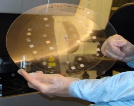
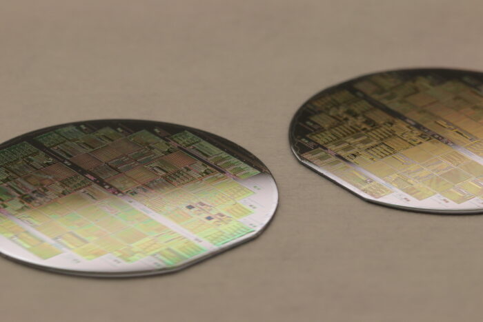
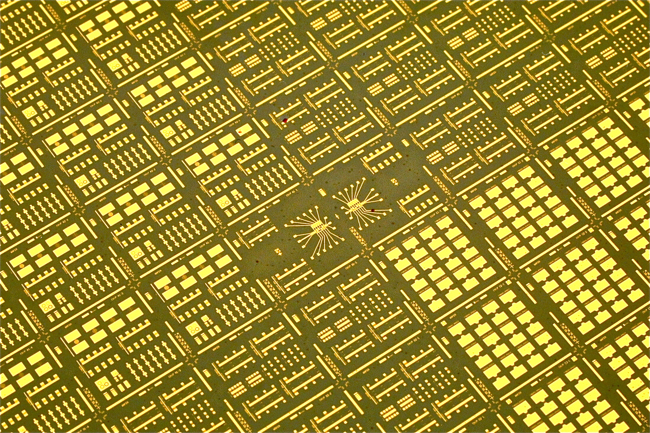
Through multi-project wafer (MPW) runs, the prototyping-cost of Si-photonics circuitry is reduced by an order of magnitude and is commensurate with typical PHOTONHUB EUROPE support project budgets. Europractice IC-service is running open MPW services on the 200mm IMEC iSiPP50G and Passive+ platforms, whereas CMP is running a similar service on the LETI platform. Further access to IMEC combined Si-SiN can be obtained in dedicated wafer mode. Access to the VTT technology is possible either in an MPW-mode or in a dedicated run mode. Same can be said for the 6 inch line of SSSA/Inphotec, that operates an industrial-grade e-beam machine. Access to ORC can be either via an MPW run or a dedicated wafer mode. The aim at ORC is to provide wafer scale prototyping that can lead onto alternative foundry processes for production. ORC can offer a multitude of SOI-platforms for traditional 1550nm wavelength silicon photonics, extending to MIR Si- photonics up to 14μm. UPV-NTC provides fast prototyping and high flexibility to prove new designs and concepts at low-cost production.
Measurement
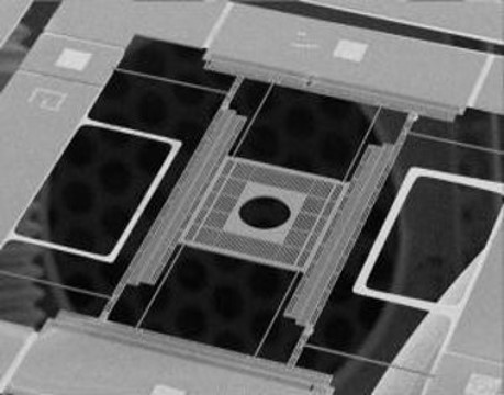
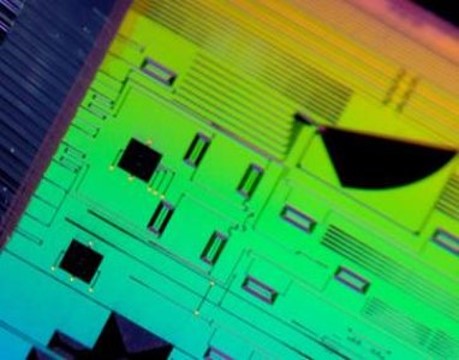
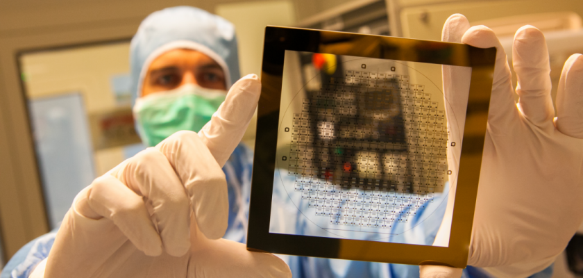
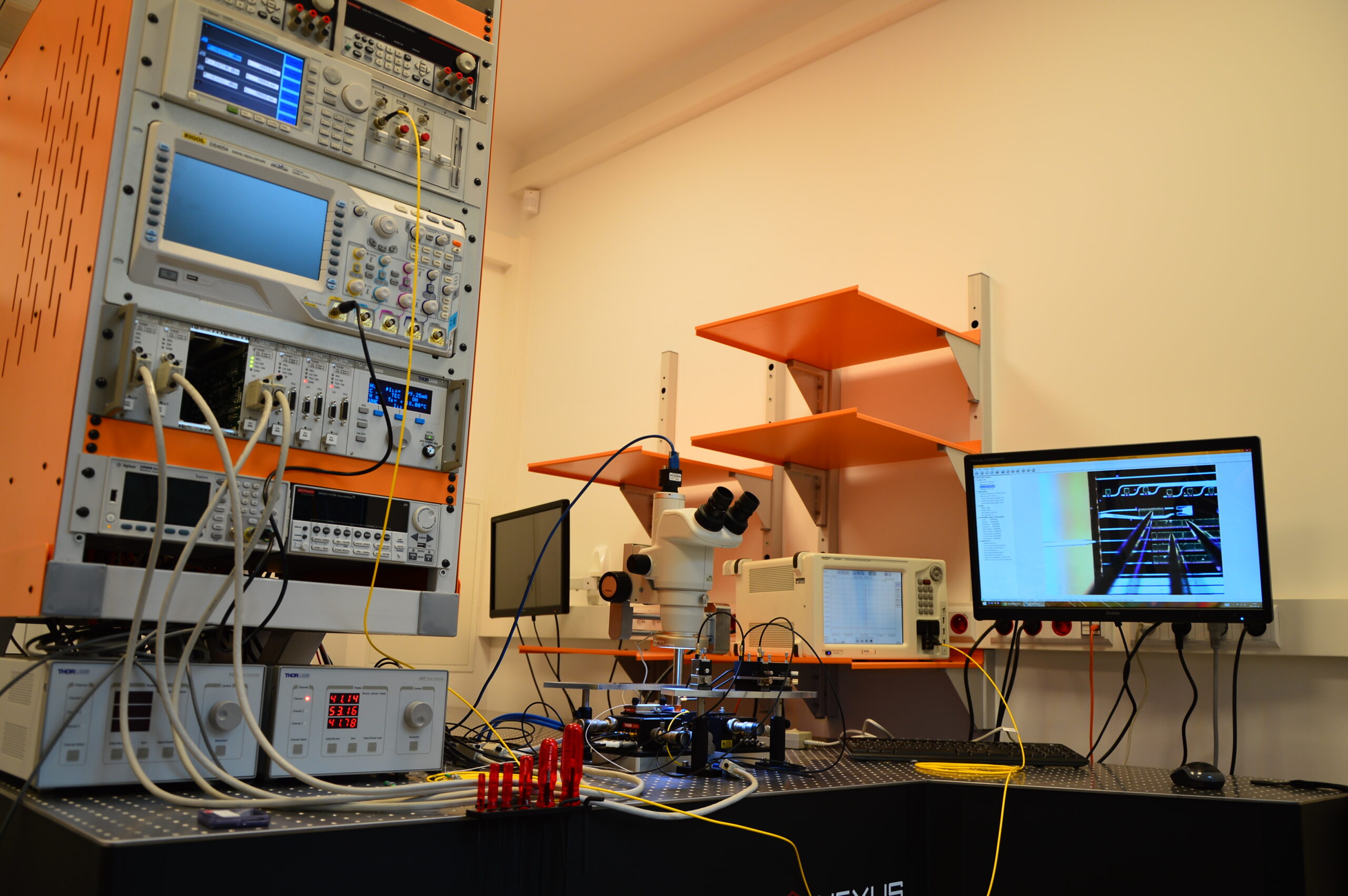
Testing silicon photonics circuitry happens at different levels. Each fab will typically include standardized test suites on each wafer that enable the monitoring of stability and performance of the platform. This approach ensures a high degree of maturity and yield of the silicon photonics platforms. In an MPW mode the testing of the specific circuits for a given project at the wafer level is unusual, because the fab will not ship wafers to the user but rather a collection of dies (typically a few dozens or possibly a few hundreds). IMEC and/or ORC have the capability to test these individual dies prior to packaging on an automated setup with respect to their basic functionality. Also more elaborate optical-electrical-high speed testing on naked dies is possible by means of optical and RF probes. This will lead to a selection of the best performing dies or circuits for packaging (typically a reticle contains multiple variants of a circuit across a certain parameter space and only a subset of them can be moving to the packaging stage). After packaging there are many options for test both at the level of the PHOTONHUB EUROPE partners as well as by the user companies. TP5 partners have capabilities for passive optical testing and high speed optical/electrical testing as well as customized testing options involving for example microfluidics
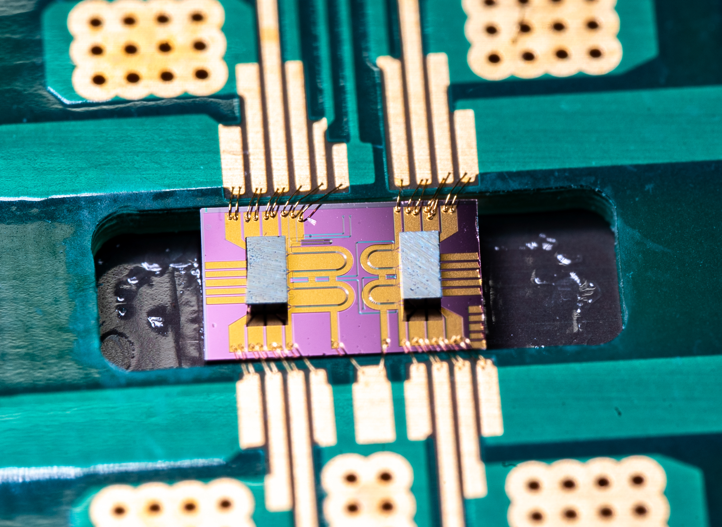
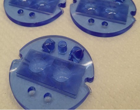
Packaging
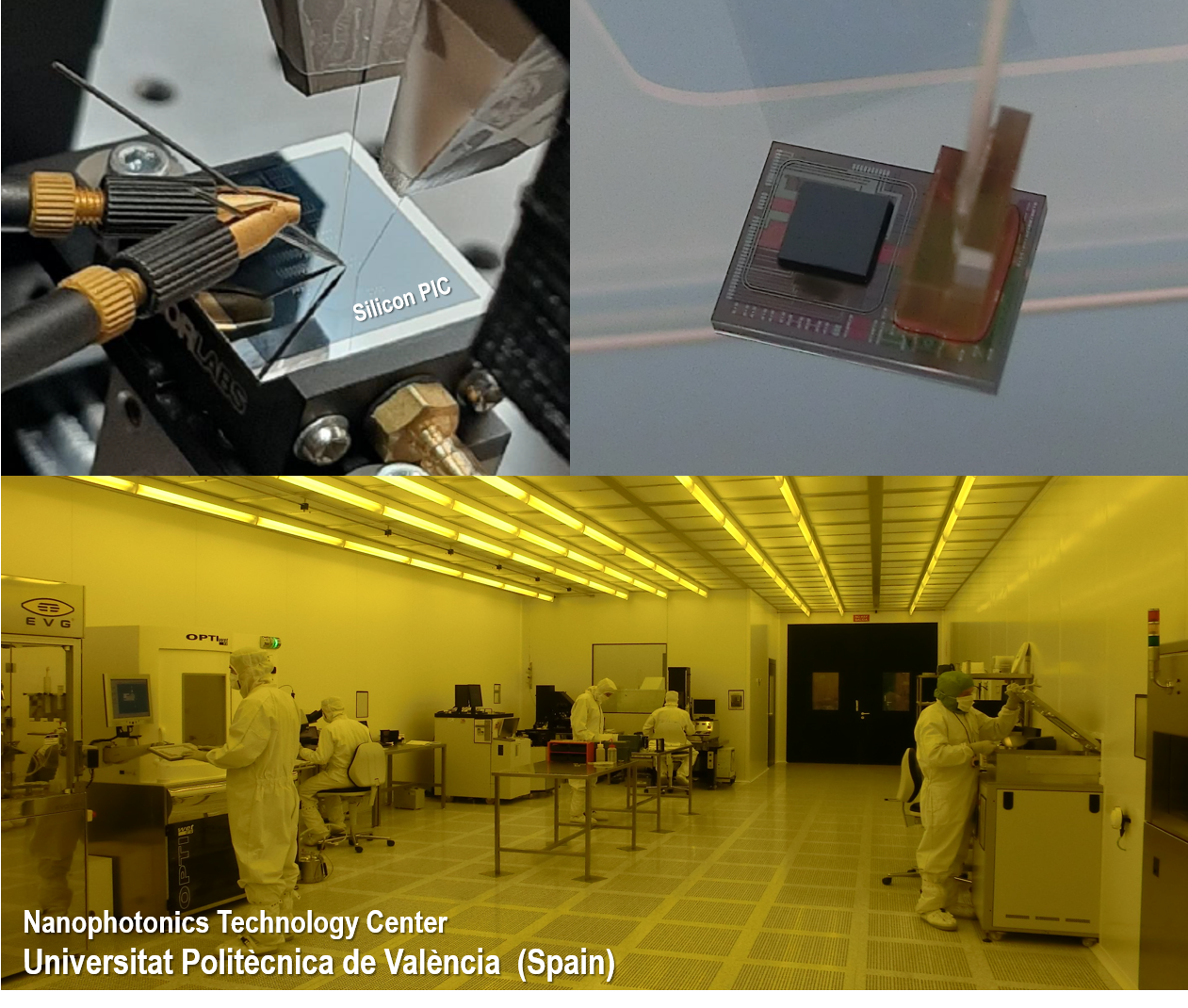
The photonic packaging capabilities provided within Actphast complement those on offer through the PIXAPP Pilot Line. Actphast partners (Tyndall, SSSA/Inphotec and UPV-NTC) have the ability to develop early stage prototypes, including fibre optics, micro optics, electrical integration, mechanical and thermal packaging. Once these early stage prototypes have been successfully demonstrated, the process can be transferred to the PIXAPP Pilot Line for scale-up, if required by the SME partner. As much as possible, standard packaging solutions will be chosen, in view of cost and maturity considerations. This is also compatible with the objectives of the PIXAPP Pilot Line.
Proof-of-concept
Through the combination of the capabilities described above a proof-of-concept demonstration will be developed that addresses the innovation need of the PhotonHub Europe user. Also, an assessment will be made about the future steps needed to bring the innovation to the market.
Reliability testing
Photonic Integrated Circuits are, by themselves, typically very robust against degradation mechanisms. Most reliability issues are packaging related. PHOTONHUB EUROPE partners have the capability to provide for a range of services in reliability testing (temperature cycling and thermal shock, humidity cycling, elevated temperature and current stress tests etc.). In most cases this will be addressed through collaboration with the packaging pilot line PIXAPP. In a typical PHOTONHUB EUROPE project preliminary reliability testing can be provided. Rigorous and extended lifetime testing will be addressed in a later development phase.