Platforms
Design
TP1 maintains a large set of both in-house as well as commercial tools for optical and mechanical design of free-space photonic components. Both rigorous methods as well as raytracing and direct design methods are available, which allows covering a complete range of photonic components: – subwavelength – diffractive and resonant gratings, computer generated holograms, waveguides and wave-optical elements, complex optical coatings towards free-form micro- and macro-optics and hybrid optical systems including opto-mechanical design and tolerancing. Thermal and stress analysis are addressed within the concept of design for manufacturability and testing. Tools for mould design and simulation are also provided as well as a variety of optomechanics, customized electronic boards, and motor control design capabilities.
Prototyping
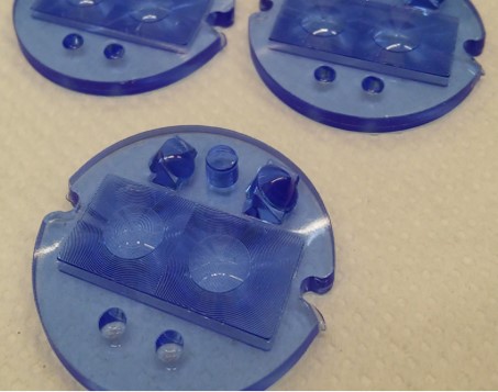
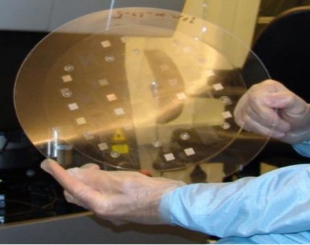
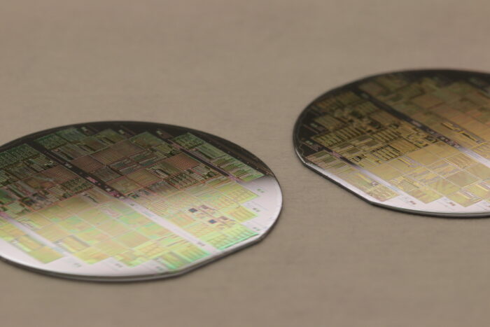
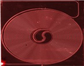
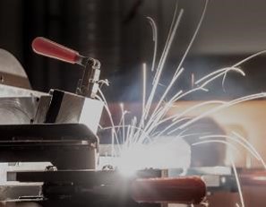
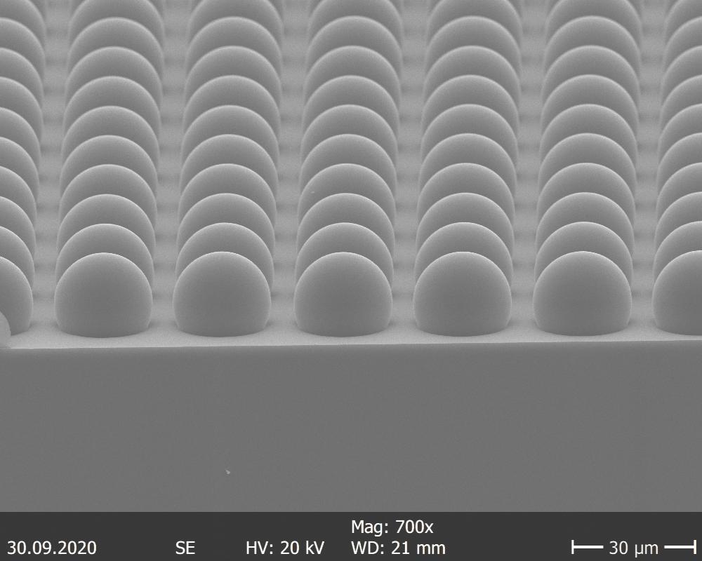
Prototyping includes one-off fabrication of optical components as well as small-series replication technologies. Prototyping can be performed in glass, using multi-axis grinding and polishing equipment, as well as in polymers by ultraprecision diamond tooling and micro-milling. (Micro-) injection moulding and various hot- and soft-embossing equipment allow for pilot production scale replication of polymer photonic components. Glass press moulding is available as well to allow for low-cost replication of low-Tg glass optics. Mastering of micro- and nanophotonics is made possible by lithography through E-Beam, UV, Nano, X-ray, and laser systems, DRIE and interference projection lithography for sub-wavelength gratings. DipPen technology for surface and device functionalization, 5 Deposition units for complex optical coatings (PARMS, e-beam, IAD,PIAD, DIBS), and 3D micro and nano (im-) printing on amongst others glass further augments the technology platform’s capabilities. A large base of materials can be processed next to polymers, glass, (non-ferro) metallic mould materials, NiP coated steel mould inserts, sol-gel materials, metal plasmonics, dielectrics, direct photopatternable sol-gel (TiO2, TiN…). Further, precision mechanics and electronics workshops for board prototyping, experience in all types of motor control, PIC (peripheral interface controllers), FPGA and microcontroller programming, and software for hardware control and interfacing is also available.
Measurement
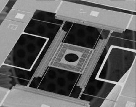
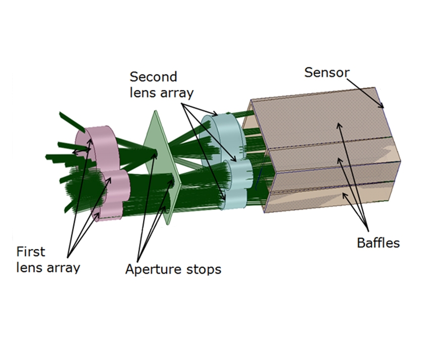
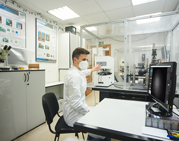
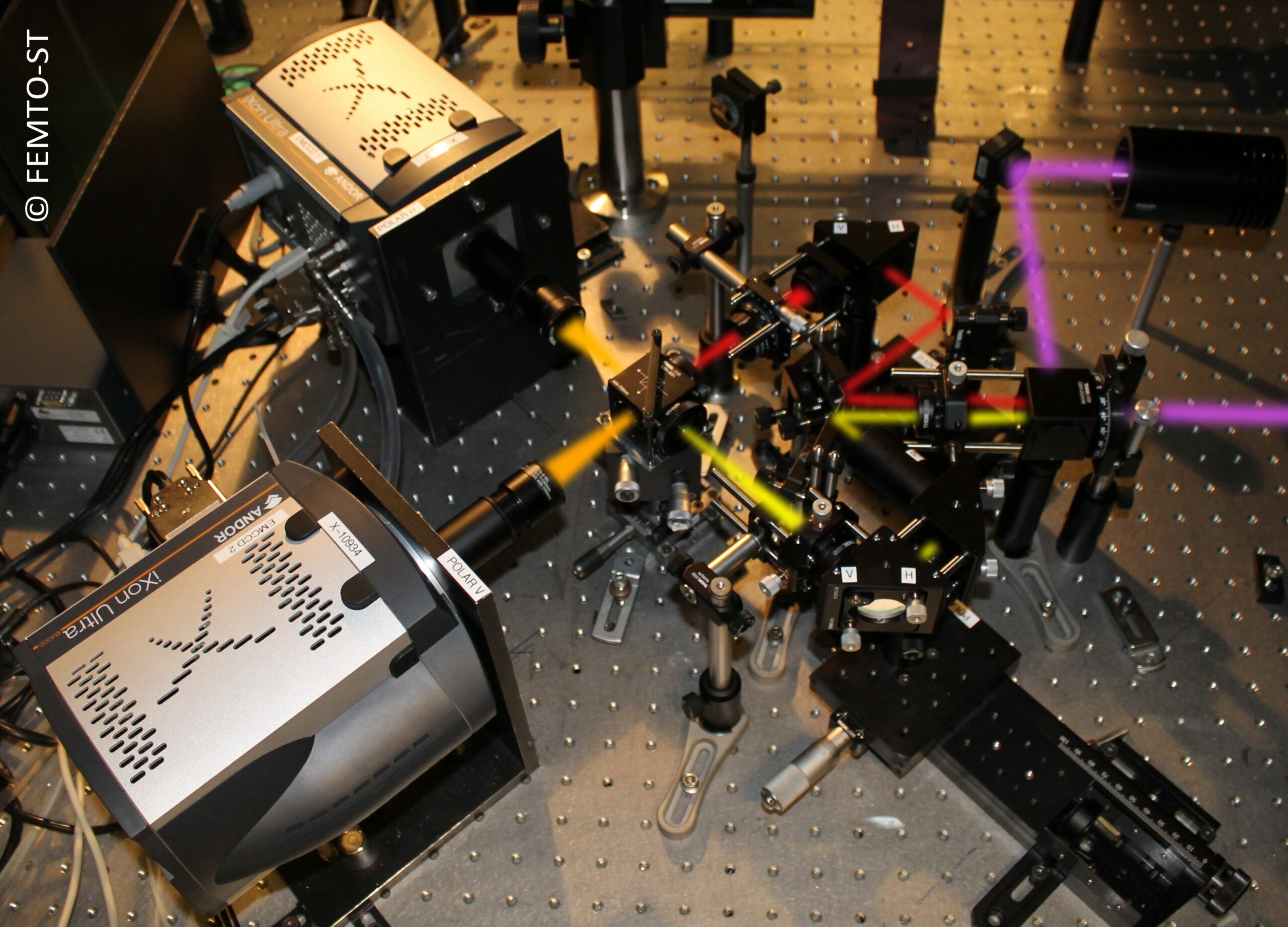
A long list of optical metrology equipment allows for in-depth characterisation of photonic surfaces, components and systems. This includes non-contact topology and lens characterisation methods based on interferometry, wavefront sensing, structured light methods, SEM, helium and confocal microscopy and tomography methods. Contact methods includes stylus profilometers, multi-sensor coordinate measurement machines and AFM systems allow mesoscale dimensioning. Vision based systems, OCT, spectroscopy, digital image correlation, digital holography further expands the measurement capabilities of the platform. Structural material characterization methods are available such as electron microscopy, X-ray diffraction & diffusion, spectroscopy, chromatography. Specular and scatter respons of surfaces and optical coatings can be characterised. TP1 has capacities in confocal microscopy, time-of-flight methods, white light interferometry, optical feedback interferometry, flow velocimetry, wavefront sensing, speckle metrology, stereoscopy, fringe projection and structured light methods, laser triangulation, photogrammetry, photometric and radiometric testing, Colour measurement, spectral source characterization, and photoacoustic imaging are available as well, together with interferometers, optomechanical sensors and Shack-Hartmann wavefront sensors. Goniometers for the residual diffusion by optical surfaces and for the characterisation of scattering surfaces, including bidirectional scattering and polarisation.
Packaging
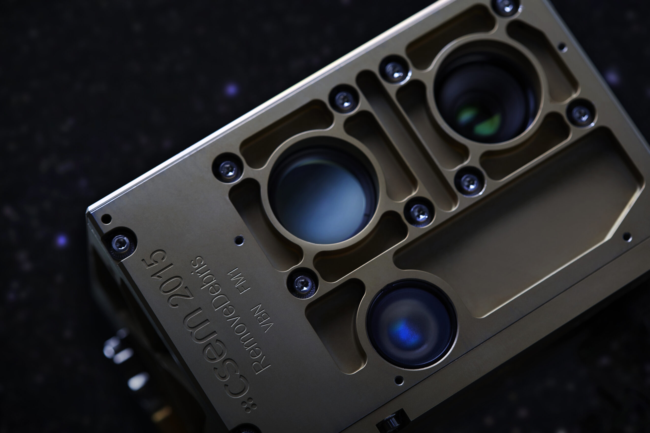
Packaging capabilities comprise the fabrication of ultraprecision parts for optical alignment, monolithically replicated freefrom optical parts, rapid prototyping of housing as well as optomechanical integration of measurement systems in application environment, large area integration using in-mould integration, R2R bonding, lamination, automated precision assembly for hybrid integration (e.g. micro-optics and fibre pigtailing), photonics and electronics module packaging and sealing (e.g. hermetic windows), optical bonding of thin substrates, 3D printing, ultrafast laser microprocessing.
Proof-of-concept
Dedicated optical testbed demonstrators for adaptive and (micro-)optics, imaging and non-imaging optics, fabrication and characterization of X-ray optical devices, biophotonic systems, optical testbed demonstrators for systems with functionalities for shape, displacement, strains, local and global features of mechanical, optical and optoelectronic structures are a number of the large amount of competences in proof-of-concept building of the technology platform. This includes replication of small series for validation and qualification purposes from consumer products to avionics and aerospace components.
Reliability testing
Reliability assessments available through the technology platform includes mechanical reliability, lifetime testing of optical devices and mechanical systems incl. thermal and fatigue tests. Climatic and environmental testing (85/85 testing or temperature cycling), vacuum and damp heat testing set-ups as well as ovens, thermostatic baths and climatic chambers allowing for accelerated ageing studies and for reliability and lifetime prediction. Also, analysis of colour reproduction, optical shop testing and wavefront sensing for quality control are available.