Platforms
Design
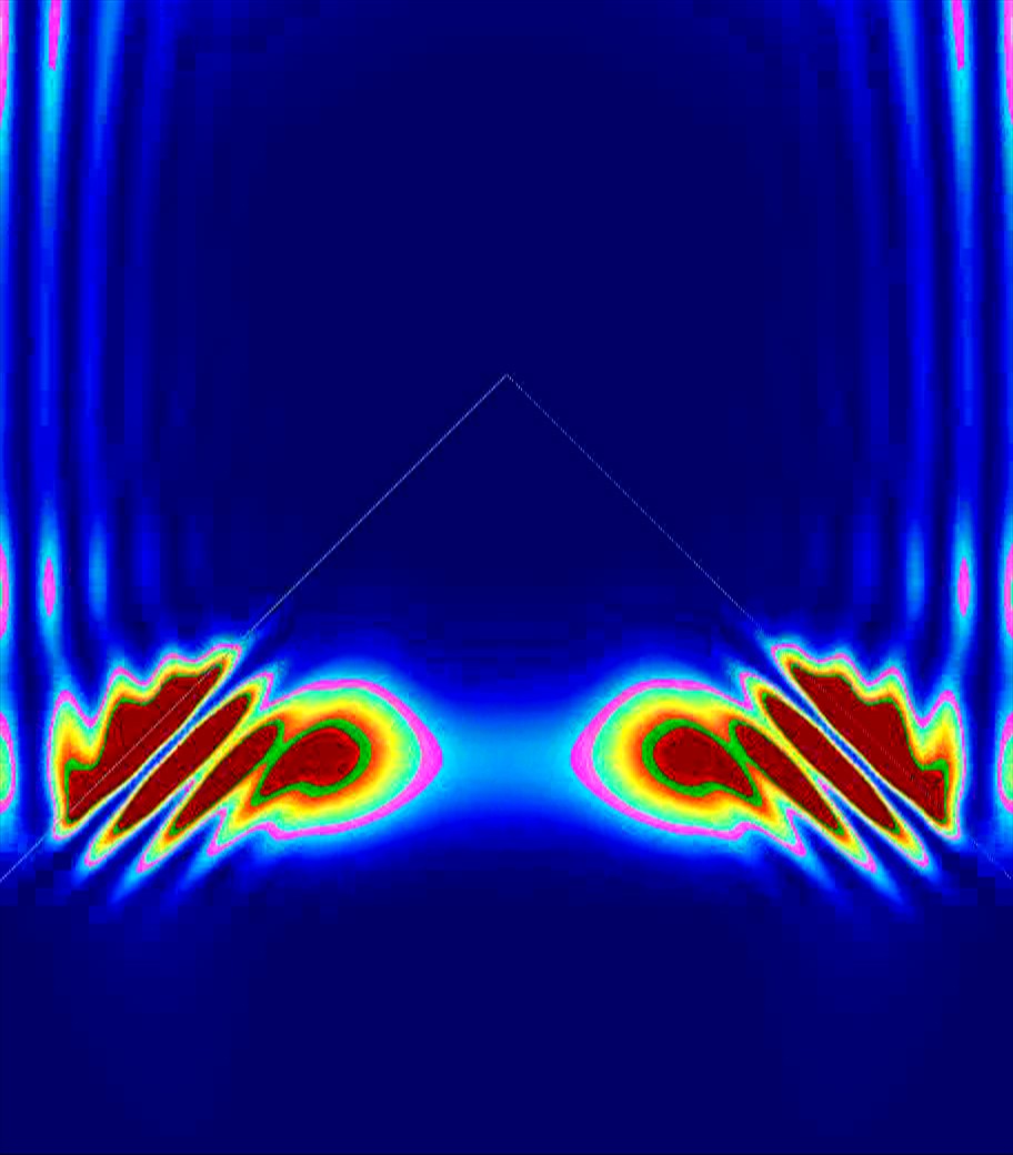
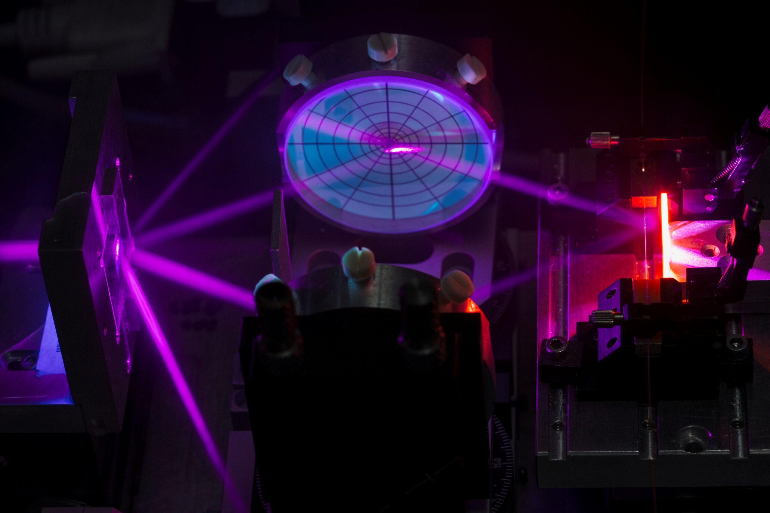
Modelling tools based on ray tracing, wave propagation methods, Finite Difference Time Domain calculation (FDTD) or Finite Element Methods (FEM), for modelling and simulation of refractive and free-form optics on waferscale, micro-optical coupling, diffractive optical elements incl. dielectric and metallic resonant gratings and coatings, nanostructured surfaces e.g. for high refractive index coating or antireflective coatings, waveguide and planar light wave circuits (PLC) modelling including simulation of light scattering; electrical and optical design modelling, of OLED, EL, OPV, OPD, light modulating structures; mechanical, optical, electrical and thermal design of photonic packages including stress analysis; modelling of processes like nanoimprint injection moulding or roll-to-roll processes.
Prototyping
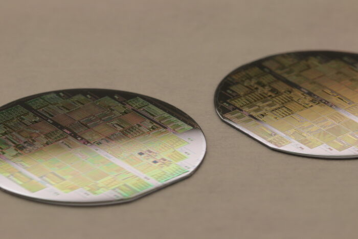
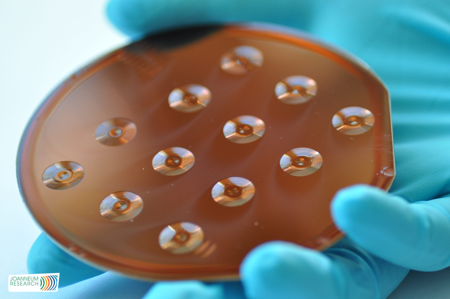
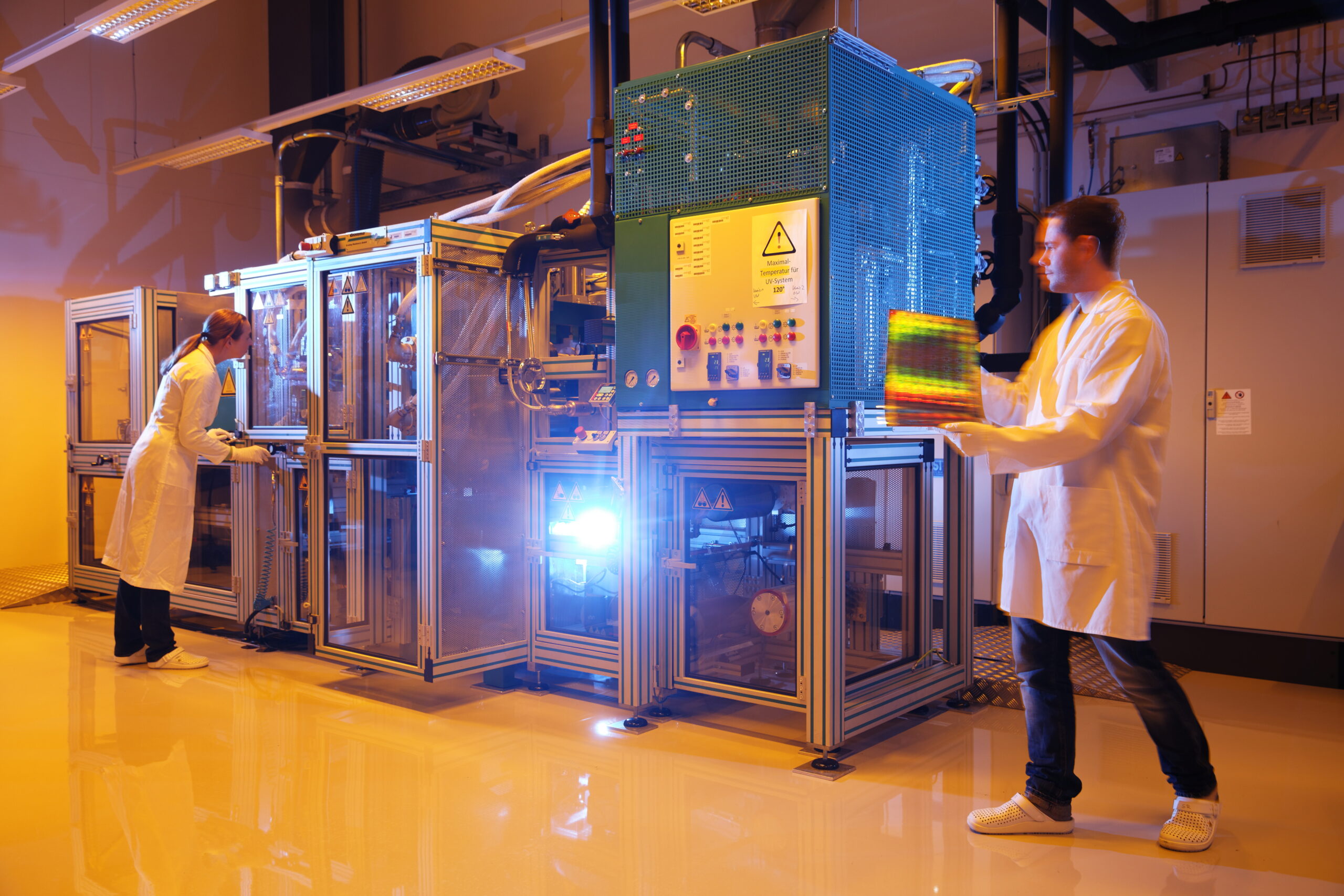
All kinds of lithography methods (E-Beam, UV incl. fringe projection, phase mask projection and grey scale, X-ray, two-photon, direct laser writing, direct photopatterning of sol-gel layers) on up to 6” substrates; replication techniques (hot embossing, injection moulding, micro- and nano imprinting, sheet-to-sheet and roll-to-roll printing, full PLC processing line up to 6”); printing techniques on large areas (inkjet, screen printing, gravure and flexographic, 3D printing in glass and polymers, hybrid printed electronics, DipPen technique); (fs)-laser micro & nano structuring and etching (wet, RIE, RIBE); ultra-precision diamond tooling and metal dewetting; thin layer technologies (ALD, PVD, CVD, PECVD, PARMS) for complex optical coatings like AR and HR layers on large area (flexible) substrates. Vacuum deposition of organic semiconducting layers in sheet-to-sheet and roll-to roll.
Measurement
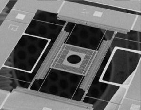
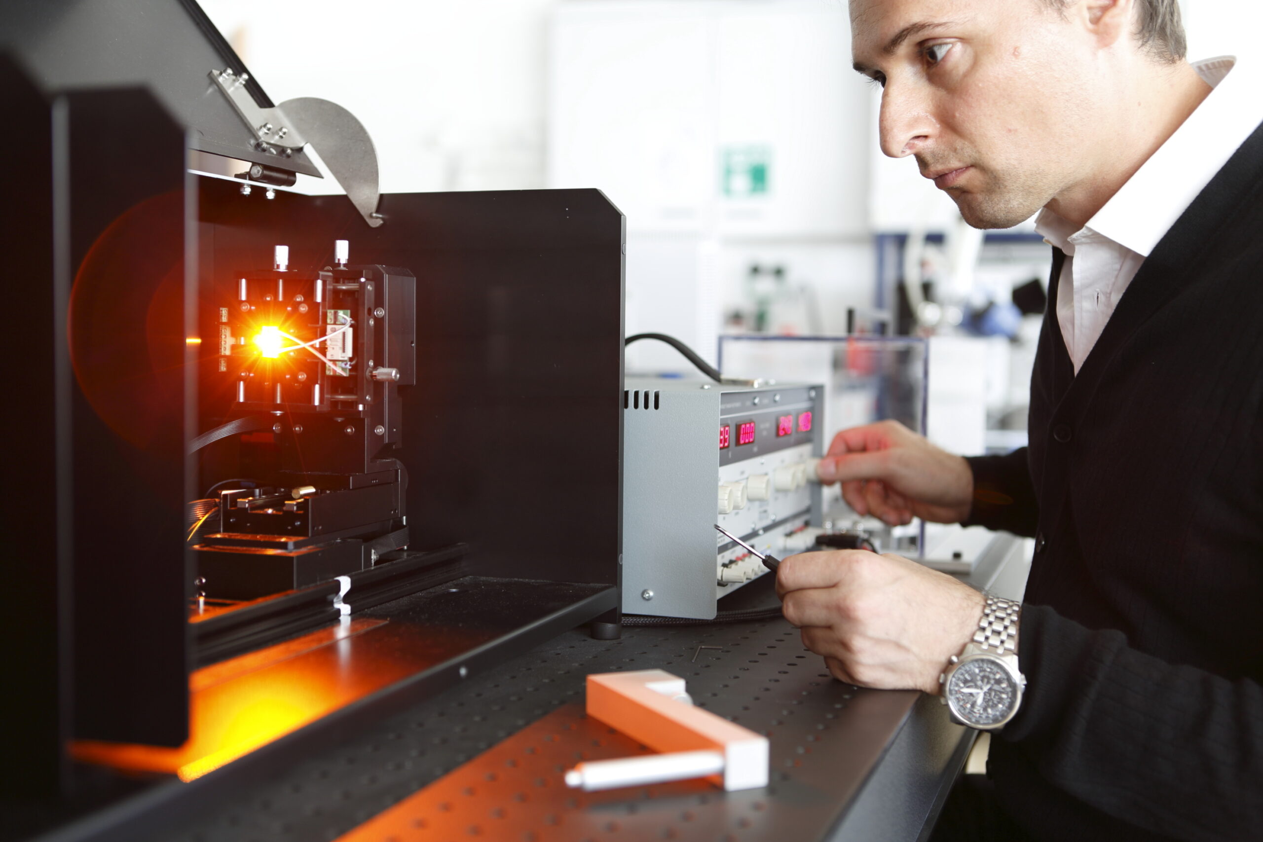
Geometry and size characterization (SEM, HIM, multi-sensor coordinate measurement, AFM, (contactless) surface profilometry, white light interferometry, roughness analysis); materials characterisation (TEM, spectroscopy incl. XPS, OCT, phase tomography, contact angle); optical characterization (reflection, transmission and holographic interferometry, refractometry, polarimetric analysis, spatially re-solved spectrophotometry, angular resolved scattering metrology, spectral charac-terisation); functional characterization (grating efficiency, beam profiling, near/far field characterization, four point e-probing, ultra-high frequency characterisation, photometric/radiometric measurements incl. Ulbricht spheres measurements;, device characterization (optical waveguides, OLED, PV, OPD); solar simulation.
Packaging
Packaging technologies are available for a variety of optical and electro-optical systems. These include: manual, semi-automatic and automatic assembly and alignment of optical components in mechanical packages, for hybrid photonic-electronic integration, hybrid integration of components into flexible plastic films, ACF bonding for flexible modules, on-chip bonding and integration, and passive fibre attachment; technologies for encapsulation like laser welding, in-mould integration, roll-to-roll bonding, lamination and encapsulation, hot pressing and film casting. It also covers passivation technologies.
Proof-of-concept
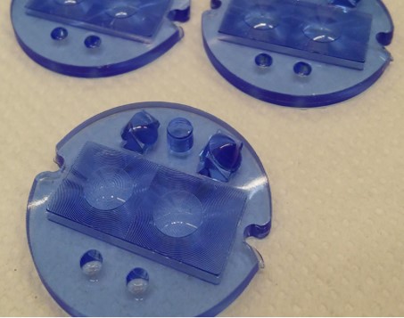
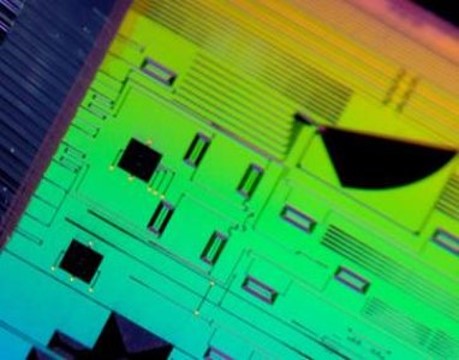
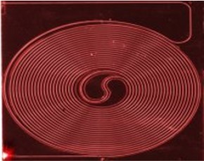
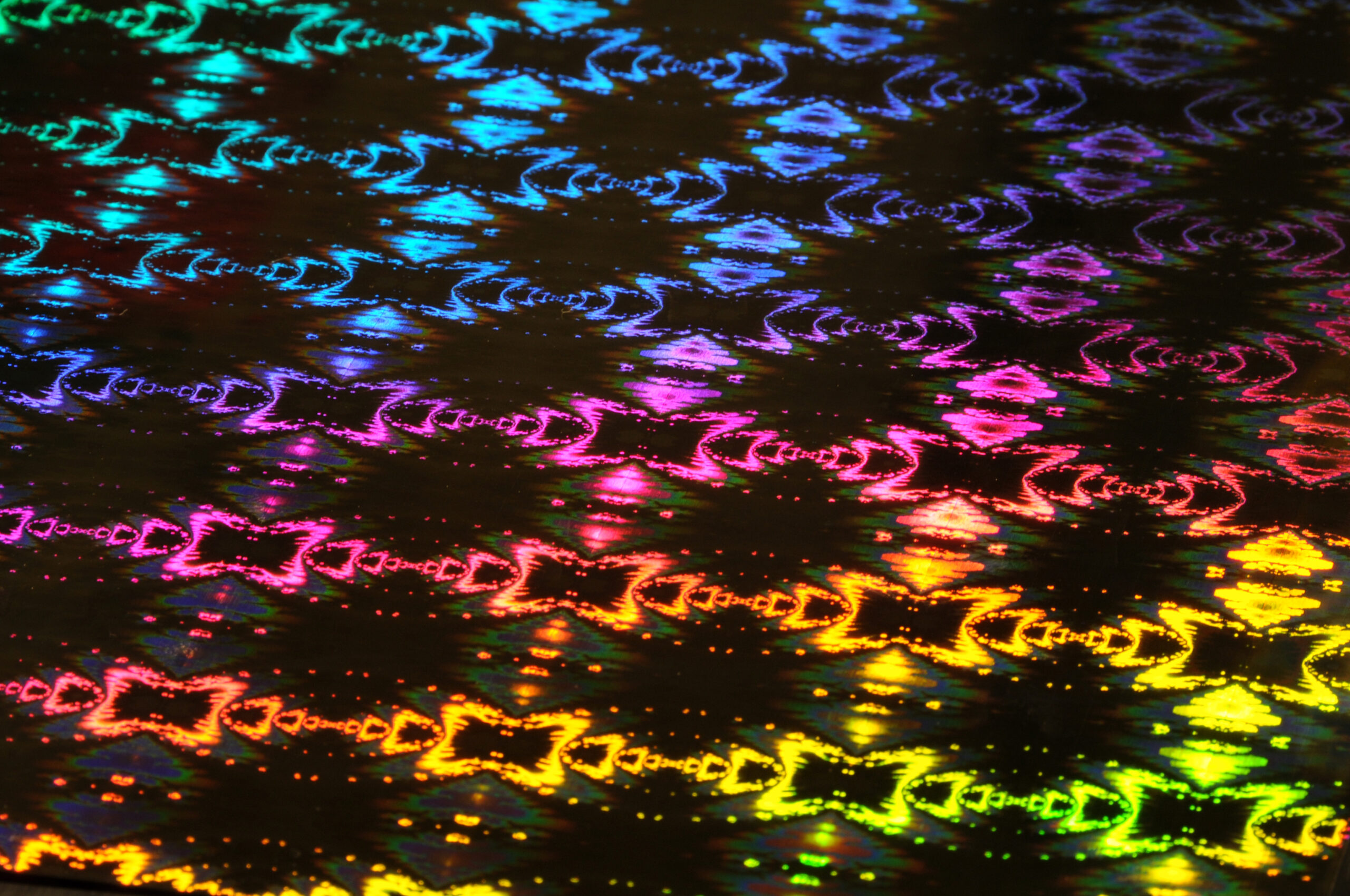
Fabrication of lab demonstrators of optical sensors (displacement, security, chemical, …), lab-on-chip for biophotonic or medical applications, imaging systems, optical filters, freeform micro-optical benches, X-ray optical devices, perovskite opto-electronics, advanced optics for photovoltaics, large area OLED, EL, OPV and OPD components like lighting foils, resonant gratings, (hybrid integrated) waveguide devices based on polymer and other platforms, m2 nanostructured optical foils and optical muiltilayers.
Reliability testing
Reliability tests under ambient conditions including thermo-mechanical testing equipment (autoclaves and climate chambers, tension/compression, bending (3- or 4-point), buckling, shock, fatigue, interlaminar shear loading, also in controlled atmospheres), friction and adhesion studies, hardness analysis (nanoindentation), cycling testing (shock, stress, temperature). OLED, OPV, EL, OPD lifetime testing.